FBGA (Fine Pitch BGA)
3D Technology - Stacked CSP
Chip on Film (COF)
Quad Flat No Lead Package (QFN)
Low-Profile Quad Flat Pack (LQFP)
Multi-Chip & Stacked Leadframe
Small Outline Package (SOP)
TSOP-I/TSOP-II
FC DFN/QFN (Flip chip DFN/QFN)
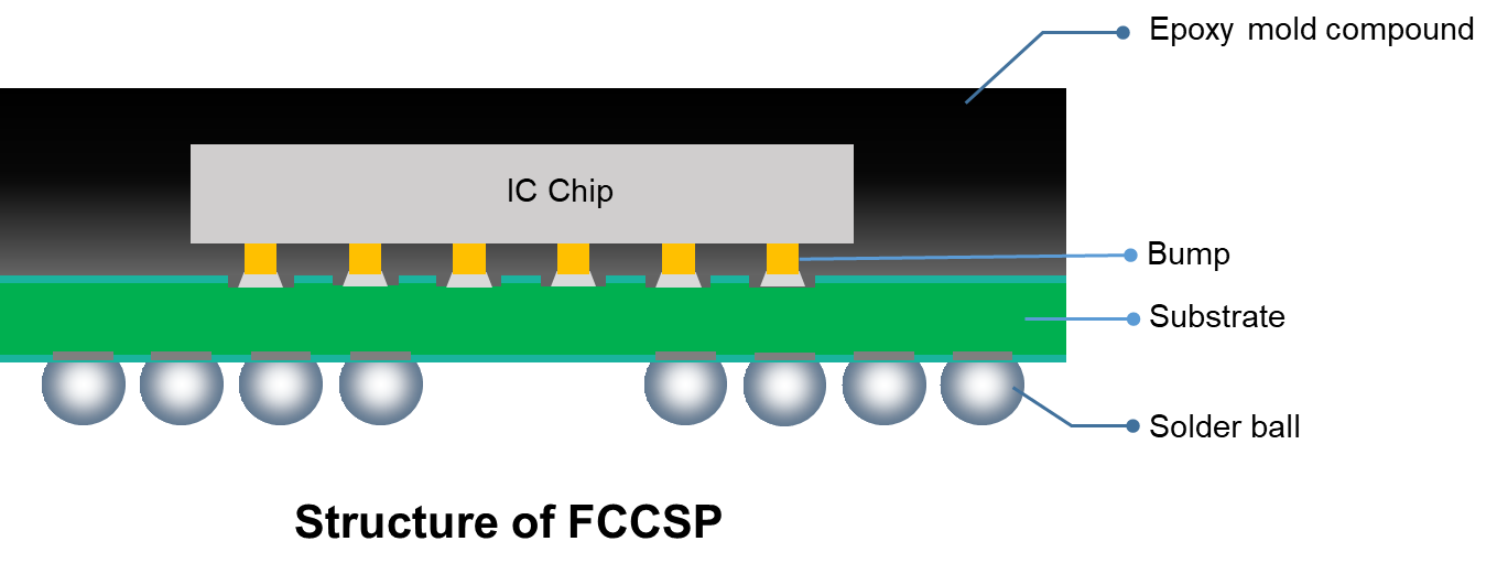
FC CSP (Flip chip CSP)
WLCSP (Wafer Level Chip Scale Package)
FPS (Finger Print Sensor)
The FCCSP package is designed as a cost-effective CSP solution specifically for high performance devices (ex:DDR V) through flip-chip interconnect technology. The structure provides the shortest connection and outstanding electrical performance through the use of bumps or balls where made of solder are formed on the wafers before being diced into individual chips. The flip-chip bump connection of semiconductor chip and substrate is designed to shorten the electric trace length as compared to gold wire in order to gain the better electrical performances and form factor.
Applications
Reliability
| Moisture sensitivity | JEDEC Level 3 | - |
| High Temp. Storage Test | 150°C | 1000 hr. |
| Temperature Cycling | -65°C/150°C | 500 cycles |
| uHAST | 130°C/85% | 100 hr. |
| Temp. & Humidity Test | 85°C/85% RH | 1000 hr. |