FBGA (Fine Pitch BGA)
3D Technology - Stacked CSP
Chip on Film (COF)
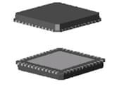
Quad Flat No Lead Package (QFN)
Low-Profile Quad Flat Pack (LQFP)
Multi-Chip & Stacked Leadframe
Small Outline Package (SOP)
TSOP-I/TSOP-II
FC DFN/QFN (Flip chip DFN/QFN)
FC CSP (Flip chip CSP)
WLCSP (Wafer Level Chip Scale Package)
FPS (Finger Print Sensor)
QFN package is a chip scale package with outstanding electrical and thermal performance. It is often used for micro controller, analogue / digital signal processors, multi-media, power management and other related devices.
ChipMOS' QFN package provides:
| Package Size | Lead counts |
| 3 x 3 x 0.75 mm3 | 10 / 16 |
| 3 x 4 x 0.55 mm3 | 8 |
| 4 x 4 x 0.65 mm3, 4 x 4 x 0.75 mm3 | 24 / 28/ 32 |
| 5 x 5 x 0.75 mm3, 5 x 5 x 0.85mm3 | 28 / 32 / 36 / 40 |
| 6 x 6 x 0.75mm3, 6 x 6 x 0.85 mm3 | 36 / 40 / 48 |
| 7 x 7 x 0.75mm3, 7 x 7 x 0.85 mm3 | 40 / 48 / 56 |
| 8 x 8 x 0.75mm3, 8 x 8 x 0.85 mm3 | 56 / 64 / 68 / 88 |
| 9 x 9 x 0.75mm3, 9 x 9 x 0.85 mm3 | 64 / 72 / 88 |
| 10 x 10 x 0.85 mm3 | 72 / 88 |
| 11 x 11 x 0.85 mm3 | 132 |
Applications
Main applications are for hand-held devices, USB, consumer products, notebook computers, PCs, etc.
Features
- Cost-Effective, leadframe based chip scale package
- Full in-house lead frame design
- Jedec standard outline
Reliability
| Moisture sensitivity | JEDEC Level 3 | - |
| High Temp. Storage Test | 150°C | 1000 hr. |
| Temperature Cycling | -65°C/150°C/15min | 1000 cycles |
| Unbiased Highly Accelerated Temperature and Humidity Stress Test | 130°C/85% RH | 100 hr. |
| Temp. & Humidity Test | 85°C/85% RH | 1000 hr. |
Process Highlights
| Wafer Backside grinding | Available |
| Die Thickness | 8 ± 0.5 mil |
| Lead Finish | PPF (NiPdAu Pre-Plated Frame) (Option for Matt Tin) |
| Marking | Laser |
Shipping
JEDEC standard tray