FBGA (Fine Pitch BGA)
3D Technology - Stacked CSP
Chip on Film (COF)
Quad Flat No Lead Package (QFN)
Low-Profile Quad Flat Pack (LQFP)
Multi-Chip & Stacked Leadframe
Small Outline Package (SOP)
TSOP-I/TSOP-II
FC DFN/QFN (Flip chip DFN/QFN)
FC CSP (Flip chip CSP)
WLCSP (Wafer Level Chip Scale Package)
FPS (Finger Print Sensor)
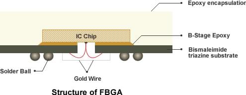
The FBGA package was designed as a cost-effective CSP solution specifically for high frequency memory devices (ex:DDR II). The structure provides the shortest wire length and outstanding electrical performance for the central-pad device layout through the use of low-cost wire bonding and BGA technologies. Generally, FBGA is defined to have the thickness of 1.2 mm and 1.0 - 0.8 mm ball pitch. ChipMOS offers several packages, including:
| Type | Packae Size | Connections |
| FBGA | 7.5 x 13 mm | 96 |
| 8 x 11.5 mm | 78 | |
| 8 x 12.5 mm | 84 | |
| 8 x 13 mm | 60/84/96 | |
| 9 x 10.5 mm | 78 | |
| 9 x 13 mm | 96 | |
| 9.5 x 11 mm | 82 | |
| 10 x 12.5 mm | 60/84 | |
| 10 x 13 mm | 96 | |
| 10 x 14 mm | 78/96 | |
| 10.1 x 11 mm | 82 | |
| 10.5 x 13 mm | 60/84 | |
| 11 x 13 mm | 60/84 |
Structure of FBGA
Applications
The FBGA package is an ideal IC package for devices such as SDRAM, SGRAM, DDR SDRAM, DDR II/III/IV/V SDRAM and next generation memory products.
Features
ChipMOS' FBGA packaging provides:
- Die-down structure
- Thin core substrate material (BT)
- Low profile (1.2 mm max. total thickness)
- Low stress die attach adhesive
- Ball pitch range from 0.75 to 1.0 mm
- Customer substrate design available
Reliability
| Moisture sensitivity | JEDEC Level 3 | - |
| High Temp. Storage Test | 150°C | 1000 hr. |
| Temperature Cycling | -55°C/125°C | 1000 cycles |
| Pressure Cooker Test | 121°C/100% RH/2 atm | 168 hr. |
| Temp. & Humidity Test | 85°C/85% RH | 1000 hr. |
Process Highlights
| Wafer Backside grinding | Available |
| Die Thickness | 10 ± 0.5 mil |
| Ball diameter | 0.45 mm |
| Marking | Laser |
| Coplanarity | < 4 mil |
| Ball Inspection | Optical |
| Packing/Shipping | Bar code, dry packing |
Shipping
JEDEC standard tray