FBGA (Fine Pitch BGA)
3D Technology - Stacked CSP
Chip on Film (COF)
Quad Flat No Lead Package (QFN)
Low-Profile Quad Flat Pack (LQFP)
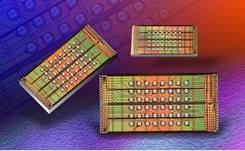
Multi-Chip & Stacked Leadframe
Small Outline Package (SOP)
TSOP-I/TSOP-II
FC DFN/QFN (Flip chip DFN/QFN)
FC CSP (Flip chip CSP)
WLCSP (Wafer Level Chip Scale Package)
FPS (Finger Print Sensor)
To meet the high demands of the growing consumer market, a Wafer Level Chip Scale Package (WLCSP) is developed. The process includes wafer bumping (with or without RDL), wafer level final test, chip singulation and packing in tape & Reel . The substrate of the package is the semiconductor die and The metallic balls provide the electrical connection from the package body to the printed circuit boards or intermediate substrates. Through this structures, it offers, higher electrical performance and best cost benefit advantages.
Applications
The WLCSP packages are suitable for mobile phones, tablets, cameras, navigation devices, game controllers, MEMS, and other portable/remote products ..
Features
- Body size range from 0.64mm2 to 25 mm2.
- Full turn-key solution include redistribution wafer bumping with or without RDL, final testing
- 4L to 116L ball count
- Low profile ( < 0.6 mm max. total thickness)
- package size = die size
Reliability
| Moisture sensitivity | JEDEC Level 1 | |
| High Temp. Storage Test | 150°C | 1000 hr. |
| Temperature Cycling | -55°C/125°C | 1000 cycles |
| uHAST | 130°C/85% | 96 hr. |
| Temp. & Humidity Test | 85°C/85% RH | 1000 hr. |