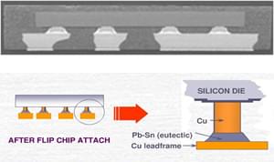
Flip chip package comprises a chip that is mounted on and electrically connects to a lead frame. The interconnection between the die and lead frame is made through an array of bumps that are placed on the bonding pads of the die surface, and then the molding compound is used to encapsulate the chip, bumps, and the leadframe.
Flip chip interconnections provide better electrical performance due to the shorter electrical path. The decrease from the die to lead frame inductances using bumps instead of wires results in lower attenuation of high frequency and fast raise signals.
| Type | Packae Size | Connections |
| FC DFN | 1 x 1.2 mm | 8L |
| 1 x 1.6 mm | 8L / 9L | |
| 1.5 x 2 mm | 9L | |
| 1.6 x 2 mm | 14L | |
| 1.6 x 2 .5mm | 16L | |
| FC QFN | 5 x 5 mm | 35L |
Applications
The Flip chip DFN packages are suitable for low lead count, and high electrical performance. The small and light package makes FC DFNs suitable for portable devices and the applications include tablet, cellular phones, wearable device and power management.
Features
- Low profile ( < 0.6 mm max. total thickness)
- Full turn-key solution include redistribution wafer bumping with or without RDL, final testing
- Improved thermal and electrical performance
- Cost effective leadframe based CSP
- Full in-house design ability
Reliability
| Moisture sensitivity | JEDEC Level 1 | - |
| High Temp. Storage Test | 150°C | 1000 hr. |
| Temperature Cycling | -55°C/125°C | 1000 cycles |
| uHAST | 130°C/85% | 96 hr. |
| Temp. & Humidity Test | 85°C/85% RH | 1000 hr. |