FBGA (Fine Pitch BGA)
3D Technology - Stacked CSP
Chip on Film (COF)
Quad Flat No Lead Package (QFN)
Low-Profile Quad Flat Pack (LQFP)
Multi-Chip & Stacked Leadframe
Small Outline Package (SOP)
TSOP-I/TSOP-II
FC DFN/QFN (Flip chip DFN/QFN)
FC CSP (Flip chip CSP)
WLCSP (Wafer Level Chip Scale Package)
FPS (Finger Print Sensor)
The FPS package was designed as a cost-effective LGA solution specifically for Finger print sensor devices. The structure provides the narrowest mold gap from die surface to package surface and high electrical performance for the sensor induction capability through the use of high DK compound and compression mold technology. Generally, FPS is defined to have the thickness of 0.4 - 0.8 mm and 0.8 – 1.2 mm pin pitch. ChipMOS offers several packages, including:
| Package Size | Connections | |
| FPS | 7.95 x 15.95 mm | 22 |
| 9.4 x 9.4 mm | 24/28 | |
| 10.4 x 10.4 mm | 12/22 | |
| 11.1 x 11.1 mm | 24/28 | |
| 12 x 12 mm | 20/22/24/26/28/40 | |
| 14 x 4.1 mm | 26 | |
| 14.4 x 6 mm | 22/26 | |
| 16 x 6.5 mm | 34 |
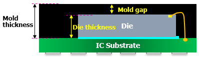
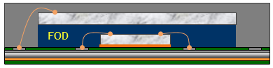
Structure of FPS
Applications
The FPS package majorly apply on mobile phone / note book / credit card as personal identification by finger print detection.
Features
ChipMOS' FPS packaging provides:
- Die-up structure
- FOD structure
- Thin core substrate material (BT)
- High DK value compound (7)
- Narrow mold gap solution (50 um)
- Package thickness range from 0.4 to 1.0 mm
- Customer substrate design available
Reliability
| Moisture sensitivity | JEDEC Level 3 | - |
| High Temp. Storage Test | 150°C | 1000 hr. |
| Temperature Cycling | -55°C/125°C | 100 cycles |
| Pressure Cooker Test | 121°C/100% RH/2 atm | 168 hr. |
| Temp. & Humidity Test | 85°C/85% RH | 1000 hr. |
Process Highlight
| Wafer Backside grinding | Available |
| Die Thickness | 50 ~ 450 um |
| Mold gap | 50 +/- 10 mm |
| Forming | Laser routing / Package saw |
| Unit warpage | < 50 um |
| Strip warpage | +/- 4 mm |
| Packing/Shipping | Bar code, dry packing, strip type |
Shipping
JEDEC standard tray