To provide customers with complete services, ChipMOS acquired Advanced Micro Chip Technology (AMCT) in April 2004 and since then ChipMOS has success fully extended its services for LCD driver from packaging and testing up stream to wafer bumping. In terms of market share, ChipMOS currently delivers more than 40% of the LCD drivers packaged in Taiwan with gold bumping technology
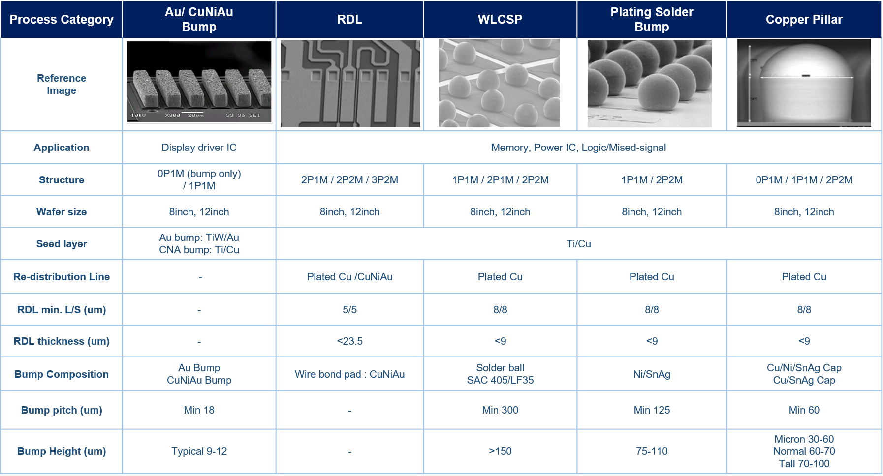
Not only gold bumping technology, ChipMOS also successfully develop and reach mass production for widely bumping services such as MCB, RDL, Copper pillar bump and Ball drop applications.
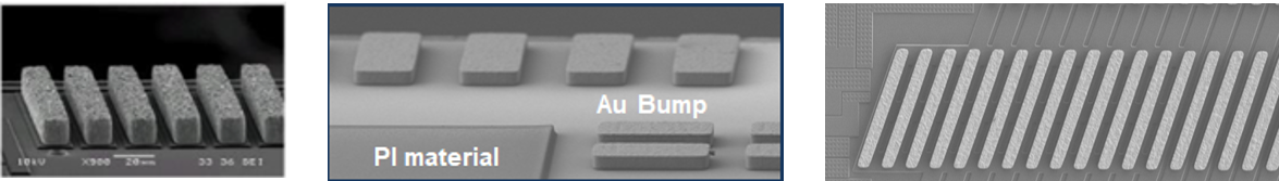
Gold Bumping
Gold Bumping technology, which is a process precedent to COF and COG packaging, is a necessary inter-connection technology for LCD and other flat-panel display driver semiconductors. Gold bump is formed on the designed I/O pads of LCD driver IC with the height of 7 - 15 um. Gold bumps play the role as the inter-connections between chips and tapes in COF packages and the glass substrates in COG package.
Gold bumping processes are available for 8 and 12 inch wafers in ChipMOS’ operations. It provides the best solution for fine pitch chips and is able to meet the high yield and efficient production requirement for LCD driver ICs, or other application chips that need low packaging profiles.
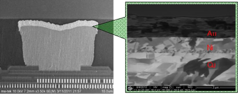
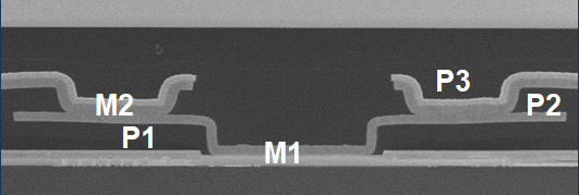
Metal Composite Bumping (MCB)
The applications of metal composite bump (MCB) are basically the same as gold bump but the bump material is replaced by a 3-layer structure of metals, instead of pure gold (Au), consisting of copper (Cu), nickel (Ni) and gold (Au). This bumping solution provides cost-competitive solutions for COG package type.
Ball Drop
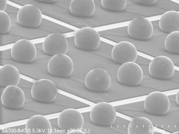
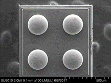
Wafer Level Chip Scale Packages (WLCSP) is a process designed to complete packaging and testing operations of semiconductor devices before wafer dicing. Normally, semiconductor devices will be placed in the carrier tape after dicing and sealed with the cover tape in order to protect the IC for subsequent processing. WLCSP provides the best solution to meet the requirements of small foot print, light weight, and miniaturization for the devices to be used in communication products like cellular phones, PDAs and other portable electronics.
WLCSP generally employ lead free solder balls to form joints with substrate in order to provide electric connections. The solder joints serve the purpose to reduce the stresses resulting from the thermal mismatch between substrate and device as well in order to enhance the service reliability.
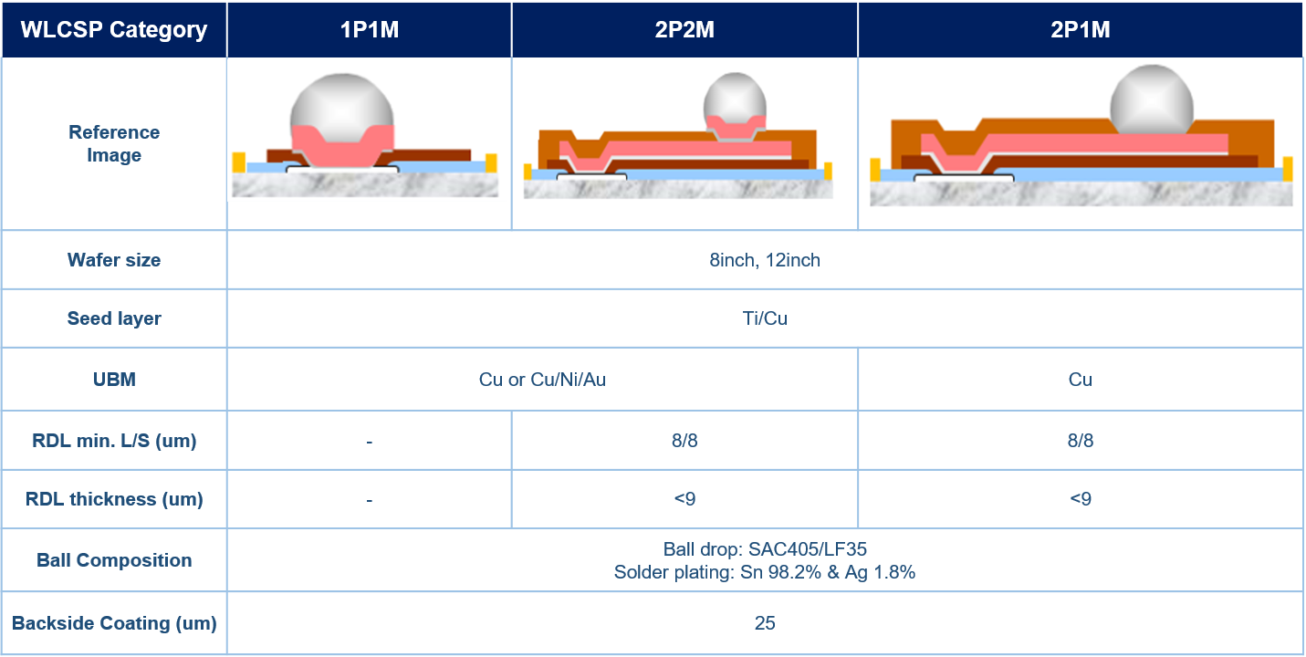
ChipMOS provides the BOP (Ball on Pad), BOT (Ball on Trace) and various solder ball composition solutions to customers. The min. pitch/diameter of ball size could be 180um/110um.
Copper RDL
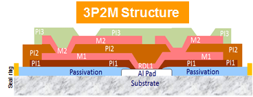
As high speed, high performance and high accuracy requirement, many electronics devices needs the capability of transferring higher current. By using Copper Re-distribution layer (RDL) technology, customer can get good electrical performance and fully leverage the footprint size. ChipMOS can provide several electroplating Cu thickness based on customer design request, including 2P1M, 2P2M and 3P2M structures. The min. size/space of RDL could be 5um / 5um.
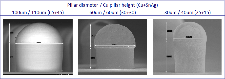
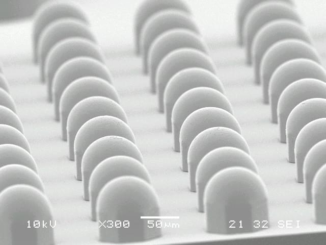
Copper Pillar
Copper (Cu) pillar is an inter-connection technology that provides better electrical and thermal conductivity, as compared to solder bump for devices with high density connections or with higher electric current.
The advantages of Cu pillar bump are as below:
- Better electrical performance (Good EM)
- Better thermal fatigue performance
- Higher elastic modulus
- Good Reliability test result
- Larger spacing between adjacent bumps for signal routing and easier underfill flow
- Lower cost
ChipMOS offers Cu pillar solutions with PI/RDL structures as well as PI-free options.