FBGA (Fine Pitch BGA)
3D Technology - Stacked CSP
Chip on Film (COF)
Quad Flat No Lead Package (QFN)
Low-Profile Quad Flat Pack (LQFP)
Multi-Chip & Stacked Leadframe
Small Outline Package (SOP)
TSOP-I/TSOP-II
FC DFN/QFN (Flip chip DFN/QFN)
FC CSP (Flip chip CSP)
FC BGA (Flip chip BGA)
WLCSP (Wafer Level Chip Scale Package)
FPS (Finger Print Sensor)
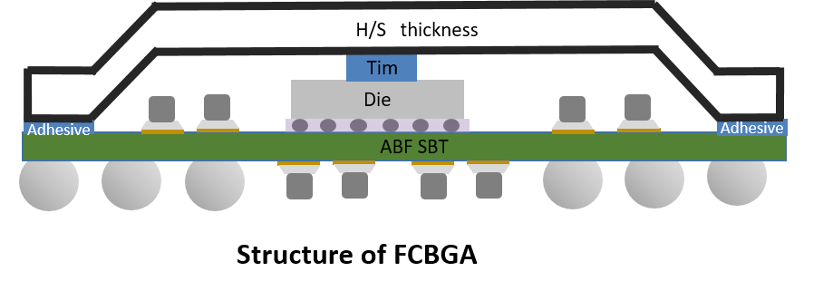
The FCBGA is an advanced semiconductor package technology that uses flip-chip interconnection. The chip is directly connected to an ABF substrate through micro bumps instead of conventional gold wire bonding. Electrical signals are routed through the substrate and finally connected to the system board through solder balls on the bottom side of the package.
Flip chip interconnections provide better electrical performance due to the shorter electrical path. The decrease from the die to lead frame inductances using bumps instead of wires results in lower attenuation of high frequency and fast raise signals.
Applications
Reliability
| Moisture sensitivity | JEDEC Level 3 | - |
| High Temp. Storage Test | 150°C | 1000 hr. |
| Temperature Cycling | -65°C/150°C | 1000 cycles |
| Temp. & Humidity Test | 130°C/85% RH | 289 hr. |